FIGURE 1.1 RS232 LINK
| Sinclair QL Service Manual | ||
|---|---|---|
| Previous | Next | |
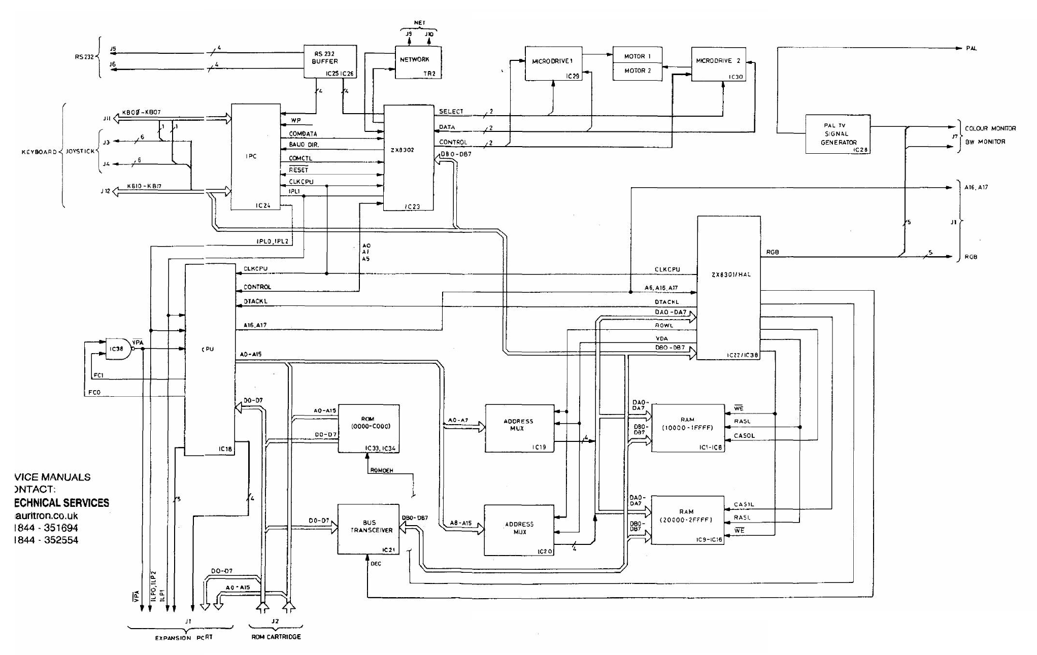
1.1 The QL computer can be regarded in hardware terms as a combination of an enhanced Spectrum microcomputer, an Interface 1, an Interface 2 and two Microdrives within the same case. In practice the resemblance to the Spectrum is small, since the QL requires two microprocessors to accommodate powerful new software and is provided with 128k bytes of inbuilt DRAM. A block diagram of the Sinclair QL is given in Figure 1.3.
1.2 Two main versions of the QL are in circulation. A certain number of boards to build standards up to Issue 5 were issued in either ROM or EPROM versions with another ROM mounted pickaback in IC33 position. The second, volume production, version of the board to build standard Issue 6, and subsequent, features 48k of on-board ROM realised in two memory devices. In the following description the two versions are referred to as the pre-Issue 6 and the post-Issue 6 versions. The main differences between the two versions, as far as the circuit description is concerned, are that IC17 and IC27 have been deleted and IC38 added in the post-Issue 6 version.
2.1 The architecture of the QL shown in Figure 1.3 incorporates much that is typical of microcomputer systems, but certain innovations make it atypical. Two microprocessors, an Intel 8049 and a Motorola 68008 are used, and the availability of 128k of DRAM plus a minimum of 200k on the two microdrives provides unusual storage facilities. The 8049 is designated the Intelligent Peripheral Controller (IPC) and the 68008 is the CPU. Two additional semi-custom ICs ZX8301 and ZX8302 control defined areas of the system, under the supervision of the CPU.
2.2 The microcomputer electronics are housed on a single printed circuit board which also houses a regulated power supply fed from an external power unit. The keyboard forms part of the upper case assembly and is connected to the p.c. board via J11 and J12. The microdrive headboards and microdrive chassis, including the microdrives and the motors, form two complete sub-assemblies which plug in to the main p.c. board.
2.3 To the rear and side of the case are plug assemblies which accommodate the following:
3.1 The Motorola MC68008 is a 32-bit microprocessor with an 8-bit data bus and is responsible for the overall timing and control of the QL. The firmware, which is outside the scope of this manual, resides in either a ROM or an EPROM depending on the version. The 68008 has an external clock, generated by the ZX8301 and has the usual bus input/output arrangement, viz. data bus, address bus and control bus. It operates semi-synchronously in this configuration.
3.2 Data Bus. D0-D7 forms an 8-bit bi-directional data bus with active high, tri-state outputs. It is used for data exchanges with the memory, with the ZX8302 and ZX8301 and with the peripherals.
3.3 Address Bus. Twenty bits A0-A19 are available for select and address purposes. A0-A15 form a 16-bit address bus with active high. The address bus provides the address for memory (up to 128k bytes) data exchanges and for data-exchanges with the QL and microdrive. Three bits A0, A1 and A5 are used for this latter purpose. Bits A16-A19 are used for device selection.
3.4 Control Bus. The control bus is a collection of individual signals which supervise the flow of data on the address and data busses. The block diagram shows most of these signals but reference to the circuit diagram shows other control signals available at the expansion port. Control lines are summarised below.
3.5 Interrupt Control (IPL0/2, IPL1). These inputs indicate the encoded priority level of the device requesting an interrupt, and are fed by IC24 (pins 23, 24) and IC23 (pin 26). A satisfactory interrupt condition must exist for two successive clocks before triggering an internal interrupt request. An interrupt acknowledge sequence is indicated by the function codes, FC0 and FC1. In this configuration FC0 and FC1 are NANDed together at IC27,6 and the output routed to the valid peripheral address (VPA) input to the CPU. This input indicates that the processor should use automatic vectoring for an interrupt. The IPL signals and VPA may also be input from an external device via J1, the main expansion connector.
3.6 A16 and A17. These two address bits select ZX8301 and are decoded by it to assert the relevant CAS0 and CAS1 signal and ROMOEH and PCENL for the ZX8302 chip enable. For this purpose their states are either low and high, or high and low respectively. When ROM is being addressed both are in the low state.
3.7 CLK Input. The CLK input denoted CLKCPU is the 7.5 MHz system clock from ZX8301. It is also fed to IC23 and IC24 and to the expansion port connector.
3.8 Asynchronous data transfers are handled using the following control signals: DTACK, R/W, DS and AS. These signals are explained in the following paragraphs.
3.9 DTACK (Data Transfer Acknowledge). This input indicates that the data transfer is completed, and is sent by the ZX8301 or through the expansion connector. When the processor recognises DTACK during a read cycle, data is latched and the bus cycle is terminated. When DTACK is recognised during a write cycle, the bus cycle is terminated.
3.10 R/W. This tri-state signal defines the data bus transfer as a read or write cycle. The R/W signal also works in conjunction with the data strobe as explained in the following paragraph.
3.11 DS (Data Strobe). This tri-state signal controls the flow of data on the data bus as shown in the table below. When the R/W line is high, the processor reads from the data bus as indicated. When the R/W line is low the processor writes to the data bus as shown.
| DS | R/W | D0-D7 |
|---|---|---|
| 1 | No valid data | |
| 0 | 1 | Valid Data Bits 0-7 (Read Cycle) |
| 0 | 0 | Valid Data Bits 0-7 (Write Cycle) |
If the CPU is addressing an external device with one of address bits A18 and A19 set, emitter follower TR8 is switched on by the signal KILLH from IC38. This sets the DSMCL (Data Strobe Master Chip - Active Low; the 'Master Chip' is the ZX8301) line permanently high thus disabling IC23 and IC22. The local DS signal is still enabled to J1, the expansion port, to control R/W operations from an external device. In the pre-Issue 6 version TR8 is switched from IC18.
3.12 AS (Address Strobe). This tri-state signal indicates that there is a valid address on the address bus.
3.13 Four other groups of control signals are used by the CPU. These four groups are routed to J1 only and are associated with Bus Arbitration Control, Peripheral Control, Processor Status and System Control in respect of external devices.
3.14 Bus Arbitration Control. An explanation of this function is included for information only. It is not used by the QL but could be used by peripherals. The 68008 contains a simple 2-wire arbitration circuit designed to work with daisy-chained networks, priority encoded networks, or a combination of these techniques. This circuit is used in determining which device will be the bus master device. The BR (Bus Request) input is wire ORed with all other devices that could be bus masters. This device indicates to the processor that some other device desires to become the bus master. Bus requests may be used at any time in a cycle or even if no cycle is being performed. The BG (Bus Grant) output signal indicates to all other potential bus master devices that the processor will release bus control at the end of the current bus cycle.
3.15 M6800-compatible Peripheral Control is exercised through the VPA and E output lines. VPA is derived from two processor status signals FC1 and FC0 as described above though this is only used for auto vectoring. E (Enable) is the standard enable signal common to all M6800 type peripheral devices. The period for this output is 10 MC68008 clock periods (six clocks low, four clocks high).
3.16 Processor Status (FC0, FC1 and FC2) are function code outputs which indicate the state (user or supervisor) and the cycle type currently being executed, as shown in the table below. The information indicated by the function code outputs is valid whenever address strobe (AS) is active.
| Function Code Output | Cycle Type | ||
|---|---|---|---|
| FC2 | FC1 | FC0 | |
| LOW | LOW | LOW | (Undefined, Reserved) |
| LOW | LOW | HIGH | User Data |
| LOW | HIGH | LOW | User Program |
| LOW | HIGH | HIGH | (Undefined, Reserved) |
| HIGH | LOW | LOW | (Undefined, Reserved) |
| HIGH | LOW | HIGH | Supervisor Data |
| HIGH | HIGH | LOW | Supervisor Program |
| HIGH | HIGH | HIGH | Interrupt Acknowledge |
3.17 System Control inputs are used to either reset or halt the processor and to indicate to the processor that bus errors have occurred. There are three system control signals: BERR, HALT and RESET.
3.18 BERR (Bus Error). Not used on the QL.
3.19 RESET and HALT. The bidirectional RESET signal line acts to reset (start a system initialisation sequence) the processor in response to an external RESET signal. An internally generated reset (result of a reset instruction) causes all external devices to be reset and the internal state of the processor is not affected. A total system reset (processor and external devices) is the result of external HALT and RESET signals applied at the same time. HALT and RESET are tied together on the QL.
4.1 The 8049, IC24, is a totally self-sufficient 8-bit single chip microcomputer containing 2 k bytes of program memory and 128 bytes of RAM. It is clocked internally at 11 MHz from crystal X4.
4.2 In this application the function of the 8049 is to:
4.3 Data Bus. DB0-DB7 constitutes an 8-bit bi-directional data bus with active high tri-state input/outputs. It is used only as input for scanning the keyboard and joysticks.
4.4 Control Bus. Control is exercised by a number of discrete signals which organise the direction and flow of data between the 8049 and the ZX8302, and also communicate with, and monitor, other areas of the QL.
4.5 Control Lines. The role of each control line is as follows:
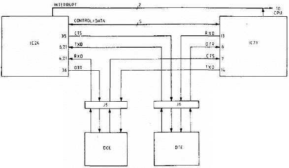
4.6 RS232 Link. IC24 is responsible for the receive side of the RS232 serial data link only, and IC23 the transmit side. Since, the RS232 link is best understood as an entity both aspects are discussed here.
4.7 J5 and J6 are two RS232 connectors. J6 is connected so that the device connected to it may act as the Data Terminal Equipment (DTE) which originates the Data Terminal Ready (DTR) signal. J5 connects to the Data Communications Equipment (DCE) i.e. the local QL assumes DTE status. Figure 1.1 illustrates this schematically.
4.8 The RS232 interface uses an 11-bit ASCII data frame, viz. one start bit, eight data bits and two stop bits comprise one character. Two stop bits are always sent but the interface receives compatibly with one except at 9600 baud, where one and a half stop bits are required. Data is transmitted asynchronously in the full duplex mode.
4.9 Consider the QL as the DTE. Both DTE and DCE are switched on and have their DTR signals asserted. CTS and DTR (Clear to Send, Data Terminal Ready) do not form a handshake pair but are similar signals going in opposite directions. Serial data is transmitted by IC23 via driver IC25/6 and received by line receiver IC26/11. From IC26/11 data is fed to NAND gate IC27/9, pin 10 of which is set to the high state by the program, and input to IC24 pins 6 and 21 via IC27/11.
FIGURE 1.1 RS232 LINK
4.10 On receipt of a start bit, IC24 is interrupted, and a subroutine clocks in the data bits, synchronised by the baud rate generator. The data, up to about 20 bytes per RS232 channel, is tnen buffered in IC24. At the same time, IC24 receives commands (and sends reports) via the serial link with IC18 which i-s controlled by IC23. When IC24 receives a command from IC18 to empty one of its buffers, it does so, down the serial link via IC23.
4.11 With the QL acting as the DCE data and control is managed in a similar way utilising different IC25 and IC26 receivers/drivers.
4.12 Keyboard Monitor. Under program control the 8049 systematically scans the keyboard, recording which keys have been pressed. Figure 1.2 shows the way the keyboard is connected. It consists of an 8 x 8 matrix with one key, the shift key, connected to three input lines. The intersection of each row and column is bridged by a normally open contact. Pressing the key closes this switch. The row 'outputs' and column 'inputs' are shown connected to separate connectors J11 and J12, one to the port 1 outputs of IC24 and the other to the data bus inputs. Pull-down resistors R17 to R24 ensure that when none of the key-switches are closed row inputs KBO0 to KBO7 remain low.
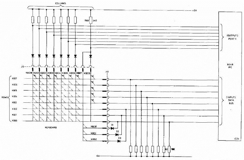
FIGURE 1.2 KEYBOARD MATRIX INTERCONNECTIONS
4.13 When the keyboard scanning routines are entered (KBOn is output, KBIn is input) the 8049 performs successive I/O read cycles setting each KBO0 to KBO7 line low in turn. At the same time the I/O port 1 inputs are scanned.
4.14 There are a total of eleven diodes used for isolation. Eight of these, D4 through D11 are isolation diodes which isolate the different rows from each other. Three of the diodes D1 to D3 provide individual isolation for the Shift Control and Alt keys so that these keys have diodes in series with them in both directions of the matrix. They are thus fully isolated.
4.15 Joystick. Connectors J3 and J4 provide a FIRE input and the four switch inputs for each of two joysticks. One line is not used. J3 and J4 are connected in parallel with keyboard connectors J11 and J12.
4.16 Loudspeaker Operation. During the execution of a BEEP instruction the IPC writes to port 2, P21 thus switching on transistor TR1 and driving the loudspeaker. The loudspeaker is damped by resistor R104 (post-Issue 6 only).
5.1.1 The pre-Issue 6 version was supplied in both EPROM and ROM forms with on-board straps enabling the selection of ROM. Both versions have 48k of ROM and in both versions there are 128k bytes of RAM memory. Figure 1.3 shows how the memory is organised.
5.1.2 The lower 48k bytes (addresses 0000-BFFF) are implemented in one 32k and one 16k byte ROM, IC33 and IC34 respectively which hold the monitor program. This program is a complex 68008 machine code program divided broadly into two parts: the operating system and the BASIC interpreter. Details of the program content are outside the scope of this manual.
5.1.3 32k bytes of memory (addresses C000-FFFF) have been left assigned to the ROM cartridge while 128k bytes of RAM (addresses 20000-3FFFF) are implemented on sixteen 64k-bit dynamic RAMs, IC1-IC16.
The following description should be read in conjunction with the circuit diagrams given in Figures 1.4 (pre-Issue 6) and 1.5 (post-Issue 6).
5.2.1 Read Only Memory. The CPU addresses the ROM/EPROM directly during memory read cycles using the address bus A15-A0. In the pre-Issue 6 version, depending on the ROM/EPROM fit, the enabling and selection pins on IC33 and IC34 are set by link selection on IC17. Links JU1 to JU6 via gate circuit IC17 are used to provide the correct signals; the link fit requirements for different ROM/EPROM versions is listed on the circuit diagram, Figure 1.4. In the post-Issue 6 version the ROMs are enabled directly by the signal ROMOEH from ZX8301.
5.2.2 RAM Memory (IC1-IC16). The sixteen RAM ICs making up the 16k x 64 bit RAM memory are organised as two matrices of 256 rows x 256 columns i.e. IC1-8 and IC9-16. Thus, separate 8-bit row and column addresses are required to access any one of the 64k locations in each section. These addresses are supplied by the CPU (68008) on address bus A0 to A15 via tri-state address multiplexers IC19 and IC20. These multiplexers decode from sixteen to eight lines and outputs enabled by the row address select line (RASL) signal from the ZX8301. The valid data address (VDA) selects the address from the CPU (via multiplexers IC19, IC20) or from the ZX8301. ROWL from the ZX8301 selects the row/column address. The R/W signal from the CPU informs the ZX8301 to expect either a read or a write cycle. For a write cycle the ZX8301 enables the write enable (WEL) line to the memory.
5.2.3 The eight bits each of column and row address are routed to both 64k sections of the RAM but the signals 'column address select 0' (CAS0L) and 'column address select 1' (CAS1L) from the ZX8301 ensure that only the required half of the memory is active. Address bits A16 and A17 from the CPU are decoded by the ZX8301 to enable the relevant CAS signal. The row address select line (RASL) signal from the ZX8301 is enabled during all read and write cycles from RAM.
5.2.4 The ZX8301 has priority when accessing memory since it must access the memory mapped display area in the RAM at set intervals in order to build up the video for the TV display. When the ZX8301 requires to access memory, it asserts the VDA signal to CPU address multiplexers IC19, IC20 and addresses RAM directly via its own address bus on pins 13, 17, 18, 20, 22, 24, 27 and 28.
5.2.5 Isolation between the two data busses D0-D7 and DB0-DB7 is accomplished using bus transceiver IC21. During ZX8301 memory cycles IC21 is disabled by negating the signal DEL from Hard Array Logic (HAL) IC38. This signal is controlled by ZX8301 signal TXOEL. In the pre-Issue 6 version, which does not incorporate the HAL, TXOEL is fed directly to IC21.
5.2.6 Refresh for the DRAM memory is accomplished during normal read cycles i.e. most rows are refreshed each time the ZX8301 accesses the memory mapped display area during picture compilation, the remaining rows are refreshed as a result of other read cycles also known to occur at regular intervals within the refresh period.
The ZX8301 carries out the following functions:
6.1.1 The TV picture generation section of IC22 operates in conjunction with the memory mapped picture display area to produce five colour TV signals suitable for driving a colour monitor. These signals, red, green and blue (RGB), CSYNCL (composite sync) and VSYNCH (vertical sync) are routed to connector J7. The RGB and CSYNCL signals are also input to IC28 which produces composite PAL to drive a domestic TV receiver. The same signals are mixed in transistor TR9 to produce a composite video signal to drive a standard monochrome monitor. VSYNCH is also routed to IC23 where it is used to provide an interrupt at the frame rate. This is used to give a time reference to the job scheduling supervisor in the operating system.
6.1.2 Using the 15 MHz crystal clock, X1, IC22 derives line and field timing compatible with the external receiver. Video is derived by accessing the memory mapped display area in the RAM in a set sequence at set times throughout the picture frame. The addresses are necessarily independent of the CPU and appear on IC22 address lines DA0 through DA7.
6.1.3 The net result is the five video signals output from IC22 on pins 32, 31, 30, 12 and 11.
6.1.4 The RGB signals are fed to level-setting resistor divider network R48-R53 and a.c. coupled to RGB-to-PAL converter IC28 on pins 3, 4 and 5. The composite sync signal CSYNC is input on pin 2. External components of the circuit provide a number of clamp circuits; the luminance and chrominance signals are fed out, filtered and fed back in; the chrominance 4.43 crystal oscillator is connected; and a CR lead/lag network introduces a 90° phase shift. The crystal has a very high tolerance and does not need trimming.
6.1.5 The composite PAL signal is output on pin 9, divided down and applied to an encapsulated UHF modulator M1.
6.1.6 Master clock is divided by two in IC22 from the externally connected 15 MHz crystal X1 and distributed via output pin 7 to various destinations on the board, and to J1 the main expansion connector.
6.1.7 The system address decode signal PCENL, routed to peripheral controller ZX8302 pin 10, is derived differently on the two board versions. On the pre-Issue 6 board it is output from ZX8301 pin 39 and is derived from a combination of one of the decodes from address lines A16 and A17, and A14 (via DA6). In the post-Issue 6 version it is output from HAL pin 17 and is derived in a similar way from a decode of address lines A16, A17 and A6.
The ZX8302 is termed the peripheral chip since it controls all signals to and from the peripheral devices. Signals to/from the following are supervised:
| Keyboard | by serial link to IPC |
| Speaker | |
| Joystick | |
| RS232 (half) | |
| RS232 (half) | |
| Net | |
| Microdrive | |
| Real-Time clock | |
| Interrupt control |
6.2.1 IC23, in common with IC24, works autonomously and is polled by the CPU. It has its own 32 kHz crystal clock X2 and has an external interrupt input on pin 2 from J1, the expansion connector. Switch S3 connected to pin 21 resets the device when operated. Pin 28 output resets the CPU and IPC.
6.2.2 Address lines A0, A1 and A5 from the CPU select the specific device requiring service viz: one of (a) to (e) in paragraph 5.2 above. The VSYNCH and PCENL signals input on pins 10 and 32 have been discussed in paragraph 6.1.1 and 6.1.7 respectively. The DSMCL signal is discussed in paragraph 3.11.
6.2.3 Serial data from the various devices is converted to parallel data in IC23 and output to the data bus as DB0-DB7. Parallel data from the bus is converted to serial data and routed to the relevant device for transmission.
6.2.4 The RS232 serial link, the keyboard and the joystick operation have already been discussed in the 8049µC (IC24) section.
6.2.5 The two Net jack plugs J9 and J10 are connected in the same way as in the Spectrum Interface 1 circuit. The network is common emitter in that all stations on the network can either source current into the net or be turned off, i.e. be set in tri-state. Jack plugs are used such that those sockets which are unused serve to terminate the network.
6.2.6 When a jack is inserted in the socket it opens up a connection to a 330Ω resistor, R15 or R16, disconnecting it from the circuit. With a network set up, the two end stations would be the only ones with the 330Ω resistors in circuit. There is therefore their combined resistance, giving a pull-down impedance of about 165Ω to the circuit. IC23 contains the interface and control circuitry for the network.
6.2.7 The real-time clock is run from the 32 kHz crystal X2 on pins 31 and 30. Date and time are resettable under software control. On pre-Issue 6 QLs, a trimming capacitor TC1 enabled trimming of the oscillator frequency. On the post-Issue 6 the trimming capacitor has been replaced by a fixed capacitor.
6.2.8 The remaining lines out from IC23 are the microdrive control and data lines on pins 3, 1, 19, 21, 33 and 34. These inputs and outputs are discussed in Section 7, MICRODRIVE.
7.1.1 Microdrive organisation and control in the QL is similar to that found in the Spectrum, bearing in mind that the two QL microdrives are integrated into the system and that Interface 1 functions are all executed by IC23; also the frequency is different and write protect is different.
7.1.2 Additional microdrives may be connected to the system via connector EC1.
7.1.3 Only one microdrive may be in use at any instant. The required microdrive and the type of operation, read or write, is selected under software control. During a read operation data is read from the selected microdrive tape. During a write operation the microdrive tape is erased before being written. The erase head is displaced from the write head and is timed by IC23 to sink current before the write head is enabled.
7.2.1 Microdrives are selected using the MDSELDH and MDSELCKN signals from IC23. Each microdrive control chip, IC29 and IC30, contain one stage of a shift register, realised by a flip-flop. MDSELCKN is connected to each microdrive and MDSELDH is routed to pin 22 (COMMS IN) of IC29, which is the input to the shift register. The shift register output on pin 20 (COMMS OUT) is routed to COMMS IN in IC30. COMMS OUT on IC30 pin 20 is routed to microdrive expansion connector EC1. The selected microdrive has a '1' on its COMMS OUT pin. Thus the required microdrive is selected by shifting the '1' accordingly.
7.2.2 COMMS OUT not only feeds the next microdrive; it is used to select its own chip internal functions and to select the LED, the motor, and the erase current for the selected microdrive. Therefore while this signal is low the motor is disabled, the LED is off, no current can flow through the microdrive switch (S1 or S2), and no erase current can flow.
7.2.3 Consider the motor drive circuit for number 1 motor. A high on pin 20 of IC29 turns on TR4. This pulls the base of TR6 low, turning it on and switching power to motor 1. Capacitor C21 and resistor R28 time constant ensures that the motor does not cut out too quickly and damage the tape. The red LED D20 is switched on at the same time. With TR6 turned on and write protect switch S1 closed the erase head current circuit is enabled via pin 6 of headboard 1 connector. When the erase output is enabled on pin 1 of IC23, transistor TR3 switches on and current flows in the selected microdrive erase head. Diodes D18 and D16 provide protection against reverse currents. Diodes D12 across the erase head and D15 perform similar functions. The amount of current flowing in the erase head is limited by R25.
7.2.4 Write protection is achieved by the action of the microswitch on the microdrive chassis. The switch is operated by the write protect tab on the microdrive cartridge. When the tab is present the select supply line is connected to the erase coil, enabling the QL to write normally. When the tab is absent, the supply to the erase head is disconnected, and the MDRDWL line is held high (read mode) via R100/101 and D22/23 (see Section 5, para 3.1). This line is clamped to 5 volts maximum by diode D29. The purpose of D22/23 is to prevent unselected microdrives with no cartridge inserted (or with writeprotected cartridge inserted) from loading the MDRDWL line.
7.3.1 The MDRDWL signal on IC23 pin 3 places the selected microdrive in either the read or the write mode, and enables the read or the write amplifiers.
7.3.2 Data is recorded on two tracks using a standard stereo cassette head arrangement and is written in bytes, one byte to one track and the next byte to the other track. It is recovered in the same way. The tape itself is one continuous loop. Since hardware takes care of switching between tracks the software sees the tape as one doublelength single track.
7.3.3 Power to the microdrive circuits has to be filtered and IC31 and capacitors C9 and C11 are used to accomplish this. IC31 is the regulator.
7.3.4 Read Cycle. Consider IC29 and headboard 1. In the read mode the signals appearing in the two read coils inside the heads are differentially amplified through two amplifier chains within IC29. The signals are then converted to digital form to enable logic processing. The outputs from the two amplifiers, in digital form are enabled into the DATA 1 and DATA 2 outputs from IC29 on pins 24 and 19. These signals are routed to the interface within IC23 via RAH (Read and Write) 1 and 2, pins 21 and 19.
7.3.5 The signal recorded on magnetic tape is at the greatest when the rate of change of the signal imposing it is at its fastest. Therefore when a squarewave has been written, the greatest recovered voltage is obtained on the edge of the pulse. Since the object of the exercise is to produce a waveform which changes at the peaks of the recovered signal, IC29 contains amplifiers to bring the signal up to the required level, and a peak detect circuit which changes state when the input reaches its greatest level. The peak detector is followed by a hysteresis circuit which ensures that the output does not change on spurious signals.
7.3.6 The gain of the circuit should not need to be changed, as only one type of high quality video tape is used. The reproduced signal levels may be read across capacitors C15 and C17 and are typically in the order of 400 to 500 mV and 250 to 350 mV for the low frequency and high frequency signals respectively. In the record mode the modulator in IC23 converts the ones and zeros in the data into FM (frequency modulation) where there is always a transition at the beginning of the bit cell. If the data is a one there is a transition at the beginning and in the middle of the bit cell, which means essentially that the frequency doubles if the data contains ones. Hence high and low frequencies at C15 and C17.
7.3.7 Write Cycle. When the MDRDWL signal from IC23 goes low the selected microdrive is placed in the write mode. This has the effect of changing DATA 1 and DATA 2 on IC29 from outputs to inputs. These inputs are used to drive current sources for track 1 and track 2. When DATA 1 is high for example, current is pulled in one direction through the head, when it is low current is pulled in the other direction.
8.1 A custom-built power pack, external to the main board, supplies 9 volts d.c. at 2 amps and 44 volts peak-to-peak a.c. to the board input on connector J3. The power pack uses a thyristor to limit peak voltages on the d.c., but is otherwise unregulated and has significant ripple.
8.2 The a.c. input is applied to two rectifiers IC37 and IC36 to produce +12 volts at 80 milliamps and -12 volts at 50 milliamps, respectively.
8.3 The d.c. input is regulated down to +5 volts by regulator IC35.
8.4 All three supplies are completely protected in that the regulators are equipped with thermal and short circuit shutdown.
9.1 A good simple test of the equipment may be carried out by connecting a loopback cable to the RS232 interface connectors J5 and J6 and instructing them to talk to each other. The technique for receiving RS232 involves the data passing through the IPC, through ZX8302 and back onto the processor data bus. If this functions correctly it is close to a guarantee that the whole system is functional.
9.2 A test tape is available which exercises most of the functions of the QL and is a useful initial diagnostic tool. See Section 3 for details.
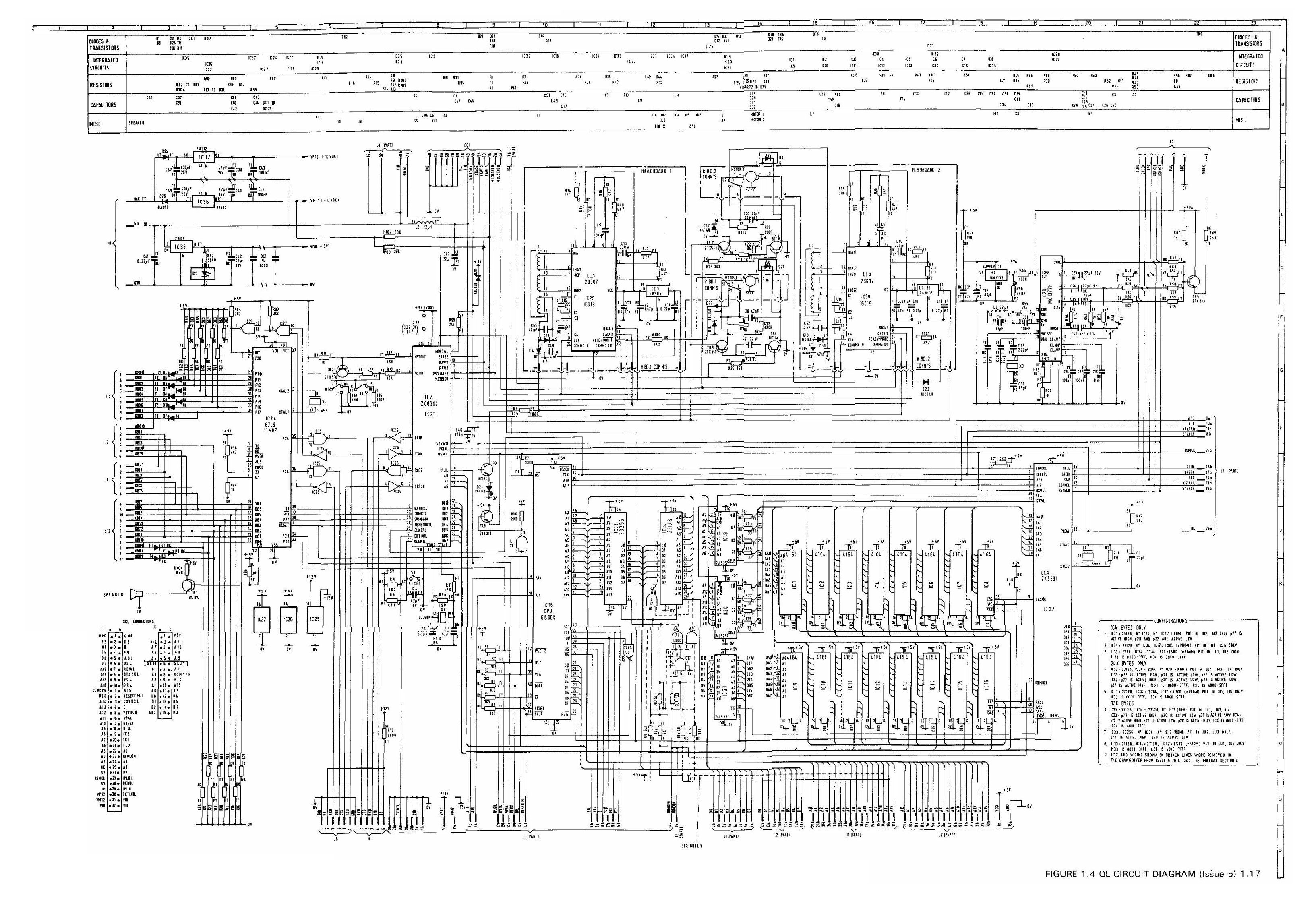
FIGURE 1.4 QL CIRCUIT DIAGRAM (Issue 5)

FIGURE 1.5 QL CIRCUIT DIAGRAM (Issue 6)
| Previous | Contents | Next |
| Contents | Disassembly/Assembly |